AMD Radeon RX 7000-Series and RDNA 3 GPUs: Everything We Know
AMD’s Radeon RX 7000-series and the RDNA 3 architecture are slated to launch before the end of the year. AMD hasn’t confirmed the name yet, but there’s little reason to expect a change from the RX 6000-series model numbers. We’re going to stick with RX 7000, though, until or unless we’re proven wrong. These new GPUs will compete with the best graphics cards, and if the third time’s the charm, AMD might even surpass Nvidia on our GPU benchmarks hierarchy.
We’ve been reporting on various rumors and leaks for months, but we’re finally close enough and have sufficient details that it’s time to gather everything together into a single RDNA 3 and RX 7000-series hub. There are still plenty of unknowns, including price and a hard release date. Specifications will continue to fluctuate a bit while AMD finalizes its plans, but there’s still plenty of data that we do know.
RDNA 3 / Navi 3x at a Glance
- Up to 96 CUs / 12,288 shaders
- 50% better performance per watt
- Double the shader count per CU
- GPU chiplet architecture
- Up to 192MB of Infinity Cache
- Launching before the end of 2022
AMD RX 7000 Specifications (Rumor)
AMD has not yet released details on the core specifications for its RDNA 3 GPUs. We do know AMD will be using “GPU chiplets” (see below), and it will also move at least some of the major building blocks to TSMC’s N5 process node, but you should view the remaining details of RDNA 3 and RX 7000 as fuzzy, at best.
Swipe to scroll horizontally
| Architecture | Navi 31 | Navi 32 | Navi 33 |
|---|---|---|---|
| Graphics Cards | RX 7900 XT, 7800 XT | RX 7700 XT, 7600 XT | RX 7500 XT, 7400? |
| Process Technology | TSMC N5+N6 | TSMC N5+N6 | TSMC N6 |
| Transistors (Billion) | ? | ? | ? |
| Die size (mm^2) | 308 GCD, 38 MCD | 200 GCD, 38 MCD | 200? |
| Compute Units | 96 | 60 | 32 |
| GPU Cores (Shaders) | 12288 | 7680 | 4096 |
| Ray Accelerators 2.0 | 96 | 60 | 32 |
| Boost Clock (MHz) | 2500? | 2500? | 2500? |
| Infinity Cache | Up to 192MB / 96MB | Up to 64MB | 32MB |
| VRAM Speed (Gbps) | 18? | 18? | 18? |
| VRAM (GB) | 24 / 12 | 16 / 8 | 8 |
| VRAM Bus Width | 384 | 256 | 128 |
| ROPs | 192 | 128 | 64 |
| TMUs | 384 | 240 | 128 |
| TFLOPS FP32 (Boost) | 61.4 | 38.4 | 20.5 |
| TFLOPS FP16 (Boost) | 122.9 | 76.8 | 41.0 |
| Bandwidth (GBps) | 864 | 576 | 288 |
| TDP (watts) | 300-450 | 200-300 | 75-150 |
| Launch Date | Nov 2022? | Early 2023 | Late 2023 |
| Launch Price | $699-$999? | $349-$549? | <$299? |
The existing RDNA 2 and RX 6000-series GPUs currently consist of four GPU designs spread out across a full dozen different graphics card models — and that’s not counting integrated graphics solutions. We may eventually see a similar lineup from RX 7000, but we’re only aware of three core GPUs at present: Navi 31, Navi 32, and Navi 33.
Logically, there will be multiple graphics card models using each GPU. AMD will also use GPU chiplets for the first time with RDNA 3, and the most credible sources indicate it will be breaking out the memory controllers and Infinity Cache from the main compute die. AMD will refer to the chips as the GCD (Graphics Chiplet Die) and MCD (Memory Chiplet Die), according to Angstronomics. Note that the smallest die, Navi 33, will retain the same monolithic design as current GPUs.
Clock speeds are mostly placeholders for now. We don’t expect AMD to walk back clocks relative to RDNA 2, and it’s possible we’ll see even higher clocks — perhaps the first GPU to break 3.0 GHz? For now, a conservative estimate of 2.5 GHz provides a rough guess at total compute. And compute… is insane.
With up to 12,288 GPU shaders each doing an FP32 FMA (Fused Multiply Accumulate) operation each cycle, that would potentially give the top model 61.4 teraflops of compute, and double that for FP16 workloads. Even the mid-tier chip would have a potential 38.4 teraflops, nearly double what the RX 6900 XT currently delivers. Which does make us wonder if perhaps these rumored specs are inflated, or if real-world throughput will be lower. We’ll find out in the coming months.
Total memory bandwidth on the top models should increase by 50% relative to the RX 6950 XT. Again, it might be more than that, but we expect AMD to stick with “vanilla” GDDR6, and the supply of 18 Gbps chips seems reasonably plentiful. Real-world memory bandwidth will get a boost from the Infinity Cache, which for most models will decrease in size compared to RDNA 2. That could be offset by higher throughput or other tweaks to the design.
There are plenty of question marks in the table for now; frankly, we could put a question mark in nearly every cell and not feel too bad about it. Names, core counts, and other aspects are all unconfirmed at present, and the only thing we know for certain is that AMD will use TSMC’s N5 node for at least some of the chiplets.
AMD Radeon 7000 Performance Expectations
(Image credit: AMD)
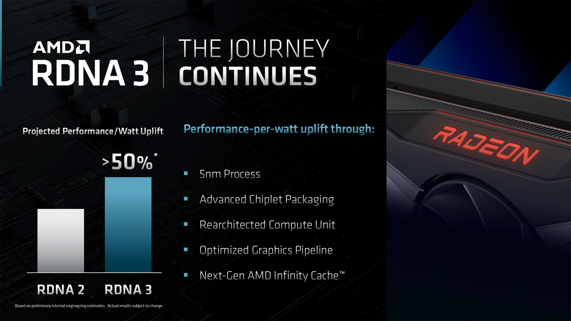
As we’ve seen with the past two generations of AMD hardware, AMD targets at least a 50% improvement in performance per watt with RDNA 3. While that might seem reasonably specific, it leaves plenty of wiggle room. For example, RDNA 2 delivered 50% better performance per watt than RDNA. Let’s give some concrete examples of how that played out.
According to our GPU benchmarks hierarchy, the RX 6900 XT consumes 308W of power while delivering 130 fps at 1080p ultra, 106 fps at 1440p ultra, and 63 fps at 4K ultra. A lower-tier RX 6700 XT uses 215W and averages 96 fps, 71 fps, and 39 fps, while the RX 5700 XT consumes 214W while delivering 74 fps, 53 fps, and 29 fps at those same resolutions.
Do the math, and the 6900 XT provides a 22% to 50% improvement in performance per watt, while the 6700 XT only provides a 29% to 34% improvement. If we add in all the other RDNA and RDNA 2 GPUs as reference points, the potential spread for performance-per-watt improvements will become even wider.
The most reasonable assumption is that the top RDNA 3 chip will deliver a significant boost to performance compared to the current top RDNA 2 chip. Considering the 50% boost to memory bandwidth, a similar or even larger boost to compute performance seems reasonable. We’ll probably see higher maximum power draw from the top model, presumably the RX 7900 XT. Lesser tier models might deliver more performance than the current generation cards while drawing less power. Your choice of resolution and setting will also impact the potential gains.
AMD has also made vague references to architectural improvements. While it hasn’t confirmed this, we expect the ray tracing hardware will get a significant overhaul. Current RDNA 2 chips use the texture units to help with BVH traversal, whereas Nvidia and even Intel have dedicated BVH hardware. Adding such hardware along with a second ray/triangle intersection unit could greatly improve AMD’s ray tracing performance. That could also contribute a lot to a metric showing a greater than 50% improvement in performance per watt.
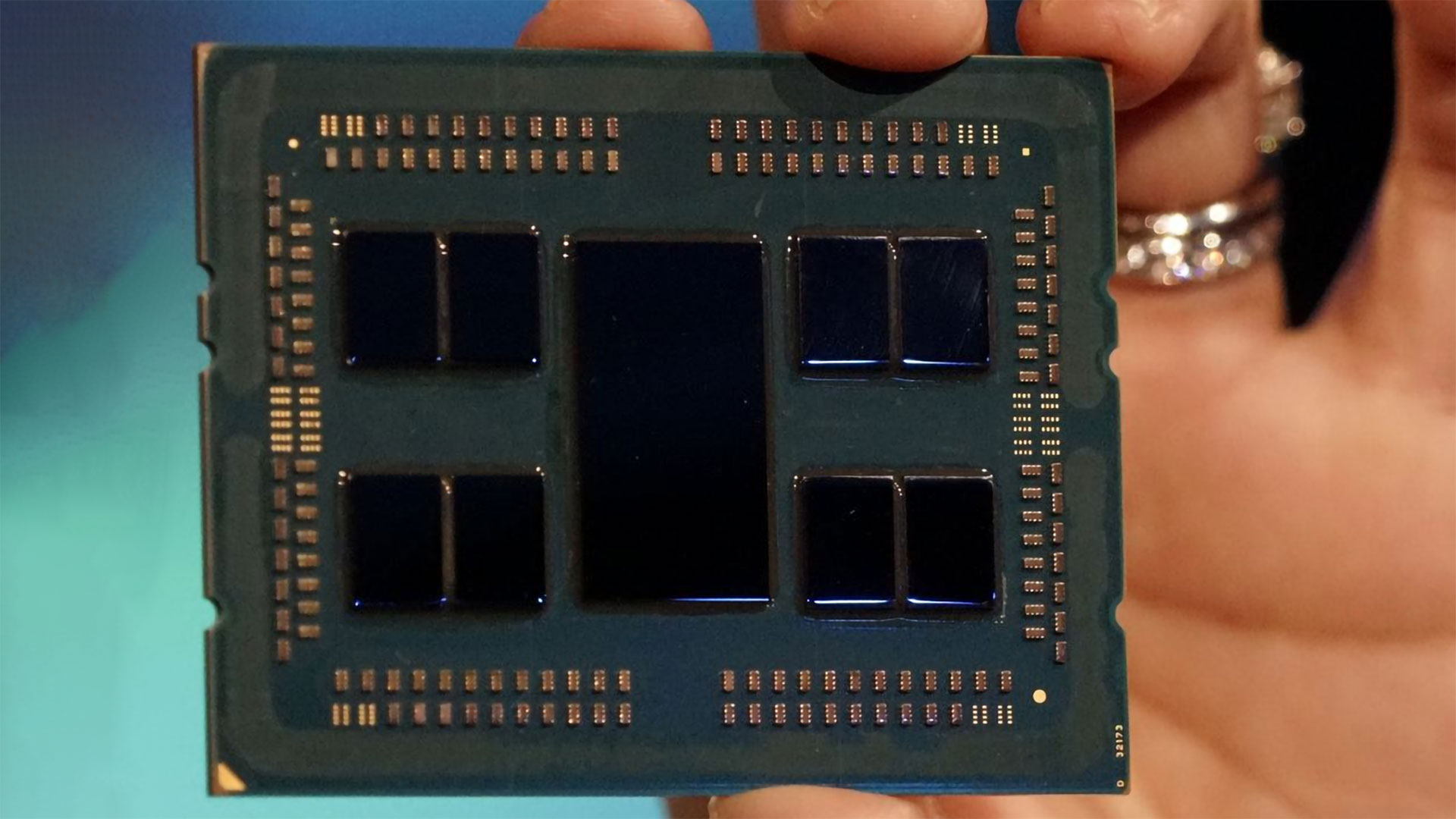
AMD RDNA 3 Architecture: GPU Chiplets
AMD’s EPYC CPUs feature up to eight CPU chiplets surrounding the central I/O chiplet. (Image credit: AMD)
One of the biggest architectural updates for RDNA 3 is something we’ve already mentioned — the move to GPU chiplets. There are a lot of good reasons for moving to multiple chiplets, though we’re still curious about the overall net benefit, which mostly seems to be about reducing cost.
Current GPU designs are monolithic, meaning everything needed for the GPU to function comes from a single piece of silicon. Because of that, GPUs build in a lot of redundancy, and chips get sold in “harvested” configurations. Navi 21 was used in the 6950 XT, 6900 XT, 6800 XT, and 6800, with up to 80 compute units (CUs) or as few as 60 CUs.
Interestingly, the Navi 21 die also has eight 32-bit memory interfaces, but AMD didn’t release any Navi 21 variants with fewer memory channels. The same mostly applies to Navi 22, Navi 23, and Navi 24 — memory and cache sizes seem to have been an all-or-nothing thing. Perhaps because the design didn’t allow for it, though Navi 22 was used in the RX 6700 (non-XT) from Sapphire with a 160-bit interface instead of the full 192-bit interface.
With Navi 31 and 32, AMD will pull all of the memory interface and Infinity Cache blocks out of the main die and move them into separate dies. Each MCD will contain a 64-bit GDDR6 interface and a 16MB chunk of Infinity Cache. Actually, the MCDs will have the option to use 3D chip stacking with another 16MB die on top of the main MCD, so they can have either 16MB or 32MB of cache. All indications are that the 32MB MCDs with stacked cache will only be used on the halo graphics card model (RX 7900 XT or whatever it’s called), but that could change over time. The MCDs will link with the GCD via AMD’s Infinity Fabric, which will see some updates to the previous variants used in Ryzen CPUs.
Breaking out the Infinity Cache and GDDR6 memory interface has some clear advantages. Transistor densities scale best with logic circuits, less so with cache, and analog interfaces (i.e., for memory) scale the worst. The on-package Infinity Fabric links on both the GCD and MCDs still require some die space, but any faulty memory controllers or cache blocks will no longer be a problem — they just get tossed.
Meanwhile, the MCDs will be made on TSMC’s existing N6 process, which costs less than the cutting-edge N5 (though N3 is coming soon), and die size won’t even be a serious concern. Angstronomics claims that the MCDs will only be about 38mm square, meaning a 300mm N6 wafer should have enough room for about 1,600 MCDs, give or take. There would be no real difficulty in simply tossing every faulty chip rather than worrying about building in redundancies.
The GCDs for Navi 31 and Navi 32 also get to be smaller, and on the costlier N5 node, that could be very helpful. AMD could still get around 180 of the larger Navi 31 GCD per wafer or nearly 300 of the smaller Navi 32. And it can still use harvested chips with fewer compute units or even MCDs to create lower-tier products.
Had AMD stuck with monolithic designs, it likely would have ended up with Navi 31 using closer to 550mm square and getting maybe 100 chips per wafer. Since N5 wafers likely cost more than twice as much as N6, this should be an easy net win from a cost perspective. It also gives AMD more flexibility with cache sizes, at least on the higher-tier products. The stacked cache is only on the MCDs, leaving the GCD free to dissipate heat into the cooling setup — that’s something 3D V-cache struggled with on its CPUs.
AMD RDNA 3 Architecture: Core Enhancements
(Image credit: AMD)
AMD will have plenty of other changes in the core architecture of RDNA 3. AMD has stated that it will have a rearchitected compute unit and optimized shader architecture, though the latter doesn’t provide much in the way of detail.
One reasonably obvious change for the GPU shaders would be to cut down on the FP64 hardware. It’s mostly there for compatibility reasons, and it costs die area. Nvidia’s consumer GPUs have 1/32 the FP32 rate and have used that ratio for several generations now, while AMD has opted for 1/16 the FP32 rate. That’s an easy fix.
The compute units will also be overhauled, and in an approach that looks similar to what Nvidia did with Ampere, we expect RDNA 3 CUs to have twice as many FP32 units. This will yield a massive boost to theoretical compute, as AMD will go from 80 RDNA 2 CUs and up to 5,120 GPU shaders to a maximum of 96 RDNA 3 CUs with 12,288 GPU shaders. Even if the real-world benefit doesn’t scale directly with theoretical compute, this should greatly improve performance.
We’ve already mentioned that we expect AMD will also be tuning and tweaking the Ray Accelerators. Sharing the texture units with the BVH traversal hardware may have been okay for the first round of ray tracing hardware, but the second generation of Ray Accelerators needs to be better. DXR performance has been one of the few weak spots with RDNA 2, and while we’re not yet at the point where ray tracing performance trumps rasterization performance, two years is plenty of time to incorporate some meaningful upgrades.
Finally, and again this comes from Angstronomics’ RDNA 3 overview, AMD will reportedly add Opaque Random Export Order to the shaders. This is apparently another die-saving technique that eliminates some extra hardware like the Re-Order Buffer.
Overall, it’s expected that the optimizations and improvements being made with RDNA 3 will result in significantly higher performance within a similar die size, even if the die were made on the same process node as RDNA 2. That’s a big claim, and TSMC’s N5 node should deliver up to a 1.8X improvement in density. RDNA 3 might even achieve such a lofty goal, given the removal of the GDDR6 interfaces and cache from the main GCD.
AMD RDNA 3 Architecture: No Need for Tensor
We asked during our interview with AMD’s Sam Naffziger whether or not we’d see tensor cores or their equivalent in AMD’s consumer GPUs. To quickly recap, tensor cores are compute cores optimized for raw throughput, with a far more limited instruction set than GPU shaders. Nvidia’s RTX cards have tensor cores for DLSS and other machine learning applications. Intel has followed suit with the Arc architecture’s XMX cores (Xe Matrix eXtensions) used for XeSS and other deep learning software.
AMD isn’t averse to providing such hardware in its GPUs, and it has tensor cores in the existing Instinct MI250X and the upcoming MI300 data center GPUs. That’s where most applications that will truly benefit from tensor cores run right now, and while there’s a potential use case on consumer hardware, AMD seems content to skip the extra AI hardware for now.
Perhaps we’ve misunderstood, and we’ll update if or when we hear otherwise. Still, AMD already has doubled the FP16 throughput compared to FP32 for tasks that don’t require higher precision. As far as we know, throughput for INT8 (DP4a) operations is again double the FP16 rate. That might not be sufficient for the fastest supercomputers doing AI training, but it does seem like it should be fine for nearly any other workload.
AMD Radeon 7000 Power Requirements
(Image credit: AMD)
Moore’s Law has largely focused on improving optimal transistor densities by reducing transistor sizes. While we continue to see progress, we’ve long since passed the point of doubling transistor counts every two years. Along with that, we’ve also seen a dramatic slowdown in power efficiency improvements.
It used to be that you’d get smaller transistors running at higher clocks using lower voltages and thus less power. Today, we get vague statements about 30% less power at the same performance or 15% more performance at the same power. Do the math, and you’ll see that those two things are not equivalent.
No company is immune to the side effects, and all signs indicate increased power consumption from the next-gen GPUs. The PCIe 5.0 power interface and upcoming power supplies that support it can supply up to 600W over a single 16-pin connector, for example, portending a broader industry shift to higher-power GPUs. We’ve heard all sorts of rumors about Nvidia’s RTX 40-series, ranging from 450W for a 4090 to as much as 800W for an extreme variant.
There’s no official word yet of TBP’s (Typical Board Power) for AMD’s RDNA 3, but it’s fair to assume they’ll push higher than with RDNA 2 on the power spectrum if that’s what Nvidia does. AMD’s Sam Naffziger confirmed as much.
“It’s really the fundamentals of physics that are driving this,” Naffziger explained. “The demand for gaming and compute performance is, if anything, just accelerating, and at the same time, the underlying process technology is slowing down pretty dramatically — and the improvement rate. So the power levels are just going to keep going up. Now, we’ve got a multi-year roadmap of very significant efficiency improvements to offset that curve, but the trend is there.”
AMD still says it has been able to drive higher clocks with RDNA 3 while remaining efficient. AMD has long discussed its strategy of ‘cross-pollinating’ CPU and GPU design teams, bringing the best tech from both sides of the house to each new CPU and GPU design. The new RDNA 3 GPU cores are supposed to be “intrinsically more power efficient,” but a business decision still needs to be made.
“Performance is king,” stated Naffziger, “but even if our designs are more power-efficient, that doesn’t mean you don’t push power levels up if the competition is doing the same thing. It’s just that they’ll have to push them a lot higher than we will.”
AMD Radeon 7000 Release Date
The only definitive statement we have on the RDNA 3 and RX 7000-series release date is what we’ve heard from CEO Lisa Su for most of the past year: RDNA 3 will come out in 2022. Time keeps ticking by, however, and with the looming launch of Zen 4 and the new AM5 platform, some groups within AMD might be spread a little thin right now.
Our take is that it makes the most sense for AMD to launch RDNA 3 once the Zen 4 dust has settled a bit. The Zen 4 launch will happen on September 27. So the earliest we’d expect to see RDNA 3 graphics cards would be a solid month after that, and it could easily be two or three months. Three months would largely amount to a paper launch, though, so hopefully, it will be in the first part of November while the big holiday shopping extravaganza is still going on.
At the same time, we’ve said for a while now that we expect RDNA 3 to echo what we saw with the RX 6000-series rollout. It will start at the top, with Navi 31 and at least two different models, possibly three. These will be the halo parts. AMD could announce Navi 32 parts as early as CES 2023 in January, or it might save those until the end of March, as we saw with Navi 22. Meanwhile, Navi 33 probably won’t arrive until late 2023.
Reusing the same MCDs with Navi 31 and Navi 32 reduces the complexity of those launches slightly, so there’s a small possibility we’ll get Navi 32 sooner than our current guess. Navi 33 will be a monolithic design, but it’s also being done on TSMC’s slightly older N6 node. Still, Navi 24 is less than a year old, so AMD likely won’t launch its replacement until 18 months have passed — which would perhaps put Navi 33 on track for a July/August release.
AMD Radeon 7000 Price Expectations
How much will AMD’s RX 7000-series graphics cards cost? This is the one everyone wants to know, and it’s also the easiest thing to change at the last minute. Assuming we’re right and Nvidia RTX 40-series cards arrive before RDNA 3, AMD will have the opportunity to react. Maybe we’ll get another attempt at jebaiting Nvidia, but it’s more likely that AMD will price its offerings in accordance with their performance.
There’s hope that things won’t be too awful this round. A glut of PC hardware is apparently gathering on shelves, from CPUs to motherboards to soon-to-be-previous generation GPUs. When new hardware launches, one of the few ways to sell the older stuff is to cut prices, but that can also have a knock-on effect on new hardware prices. “RX 7700 XT is new, but it’s no faster than the old RX 6900 XT, which I can now pick up for just $450…” That sort of thing.
Right now, it doesn’t look like we’ll have to worry so much about the influence of GPU-based cryptocurrency mining this generation. Raw memory bandwidth (i.e., not counting cache bandwidth) won’t improve too much, Ethereum should finally switch to proof of stake soon (fingers crossed, it will happen this month), and we won’t have quite as many potential scalpers sitting at home trying to figure out ways to make a buck.
Even with all the potentially good news, there’s still the simple fact that every major graphics card launch — especially new high-end offerings — has sold out. That happened with the R9 290X/290, R9 Fury X, RX Vega 64/56, RX 5700 XT, and most recently, the RX 6900 XT/6800 XT. Most of those shortages only lasted for a few weeks after the launch, with Vega and RDNA 2 being the exception, and both of those were exacerbated by cryptocurrency mining.
Bottom line: Let’s hope we’ll see a sufficient supply of RDNA 3 chips to meet early demand from high-end gamers before the end of the year.